
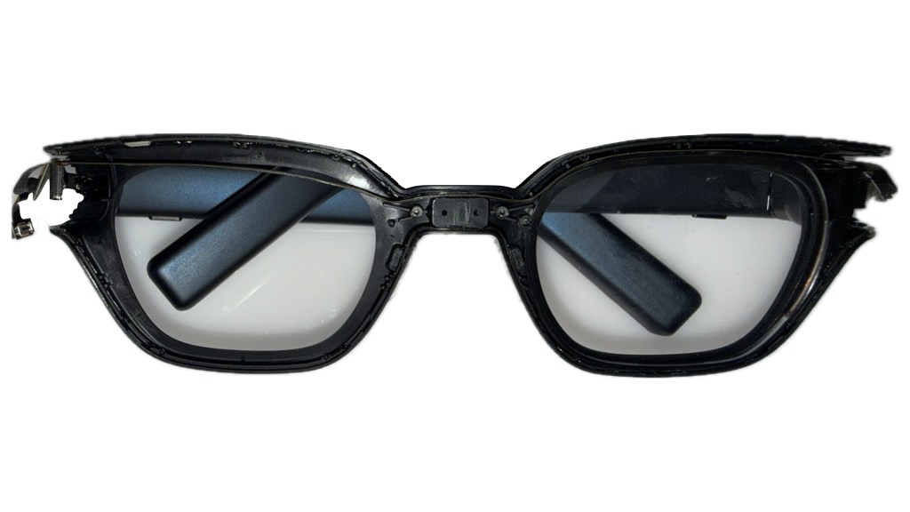
The main teardown starts with the front of the INMO Go’s, by removing the front of the faceplate (and the attached magnetic shade) and revealing the two lenses (including our waveguide in the right eye), a long flex cable connecting the two temples and an interesting cavity right above the nose bridge. The space here is interesting since it seems it is not being used despite having a dedicated volume that was molded in – perhaps INMO wanted a pogo-pin charger here, or another sensing element like a microphone, ALS or IMU, that was ultimately scrapped before production…
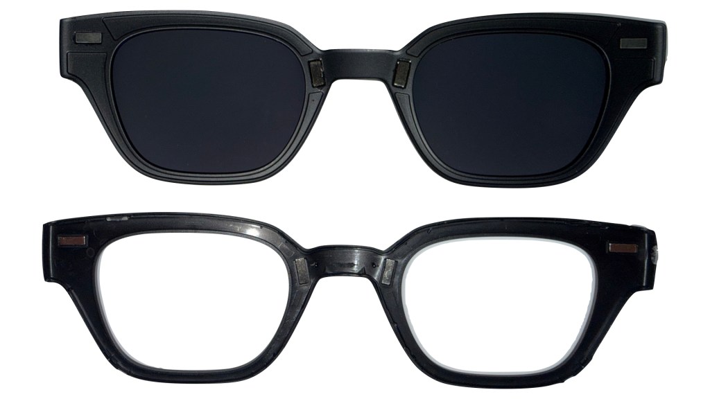
The front faceplate that we removed is a simple injected piece of plastic, but without tooling marks to tell us when it was made or out of what material… it’s likely some polycarbonate or ABS, but it would still be nice to see this in the tooling marks so that should these ever be recycled (big if), we can easily tell how to sort this resin. There are also a 4 rare earth magnets – 2 at each temple, and 2 above the nose bridge – on the inside of the faceplate that magnetically connect us to the included shade. Who doesn’t love a nice magnetic clip attachment?
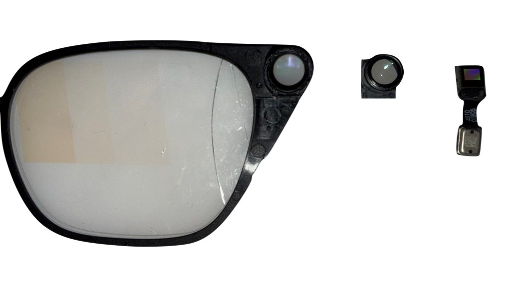
The waveguide and projector module we’ve already covered at length in the video, but here’s a quick image of the entire optical module. The JBD monochrome green projector is a two-piece module from the vendor – a green microLED 0.1″ display (right) and a single convex lens in a plastic barrel (center) to magnify the image before enters the diffractive waveguide (left) – we go into more detail on YouTube, but this is a nice static image everyone can take a look at when extremely bored.
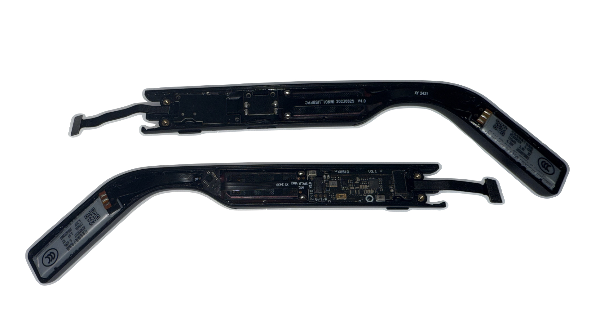
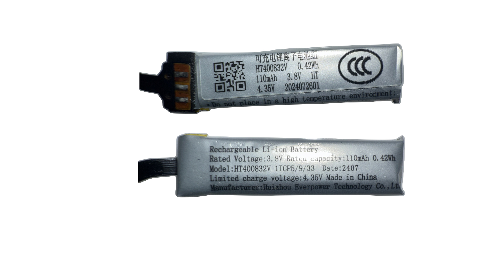
As we move to the temples, we finally start seeing the big selling point of these devices – batteries! At the rear end of each temple we have a 0.42Wh / 110mAh battery pack from a battery vendor I’ve not heard of before called Huizhou Everpower Tech. Admittedly I’ve never designed and sourced batteries, so who knows… maybe they’re a big leader in the industry outside more name-brand battery suppliers like CATL. In total, we have 220mAh of usable battery capacity, which for a highly efficient monochrome green, monocular display is more than enough for a full day of use. Especially when all processing is done on your phone (or in my case, an iPad…)
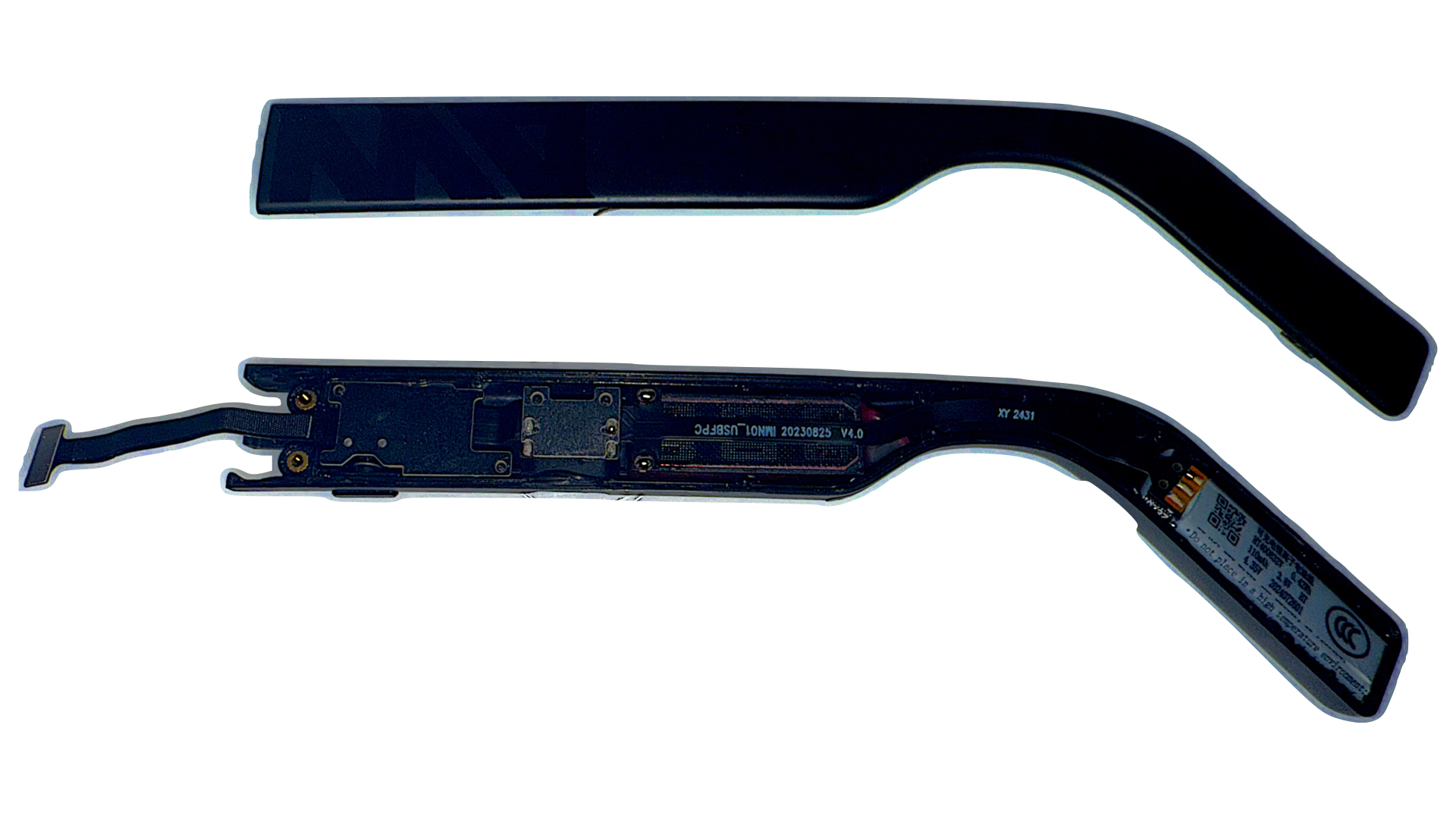
The left temple houses our USB-C input, a small PCB with the power button and it’s indicator LED, the left audio module and the left battery pack. There’s not much much to talk about here other than the frustration of seeing this single flex cable with soldered modules all the way throughout the temple… this makes small repairs a nightmare, and essentially means that any single point of failure is either a full device teardown, de-solder, and repair ($$$ – unlikely that anyone would undertake this…) or a complete device failure. Not sure what the iFixit score on this would be… 2/10?
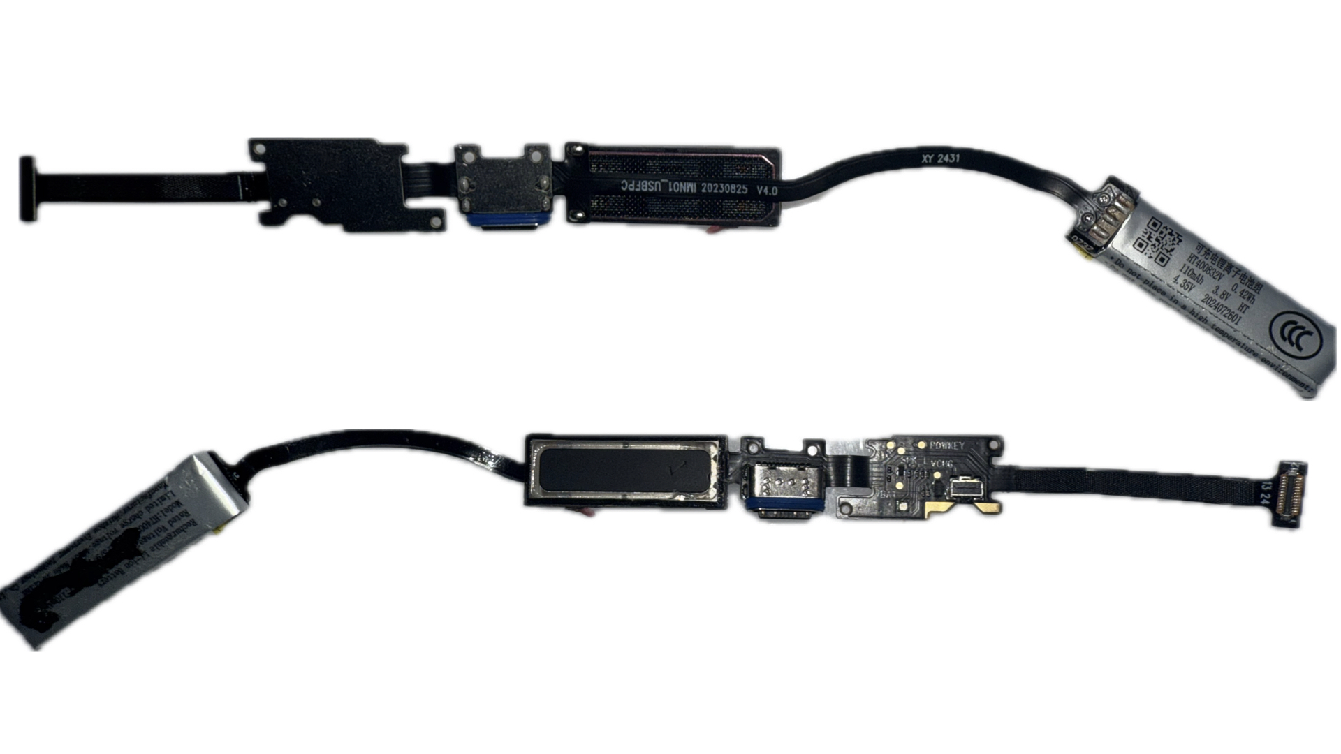
The right temple is a little more repair friendly, with independent modules and connectors for each. While everything is generally nested in the inner part of the right temple, there is one component – the touch input module – which is laminated to the outer half of the temple. I suspect we’ll see this type of component in more and more of these standalone glasses, so we’ll keep an eye for the manufacturers moving forward.
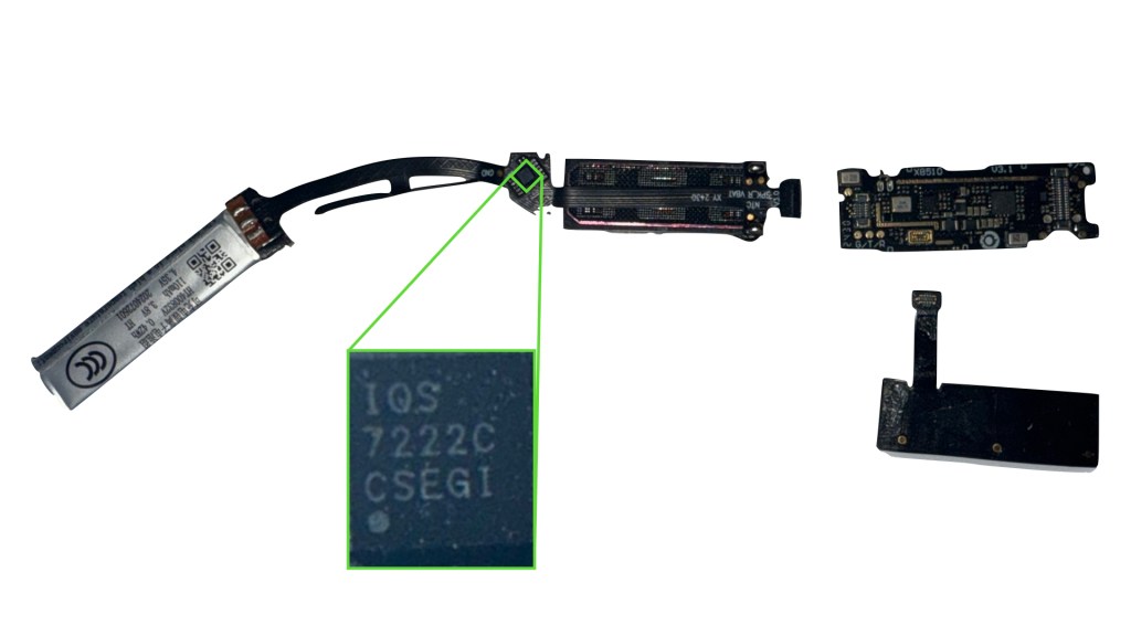
The single flex that connects the battery and audio modules to the main PCB actually has two surprising elements that weren’t seen on the left temple – a small offshoot flex between the battery and audio modules that is laminated on the bottom of the right temple, and a small IC highlighted in green. While doing my homework, I found this interesting teardown from a Chinese blogger Wen5 explaining that this part of the flex does capacitive wear detection. If true, this is an interesting low-cost solution to the battery-saving features that ToF sensing is supposed to achieve – instead of bouncing a laser on your face to see if you’re wearing the glasses, why not just see if the glasses are on your ear? It will also make it much harder for people like me to force the display on during teardowns…
The IC highlighted in green is apparently an Azoteq IQS7222C Sensor Fusion Device, meant to handle a host of signals associated with capacitive touch – this seems to just be driving and communicating the state of the wear detection flex above to the main board, which I guess is a drawback to not going the established ToF route for wear detection…
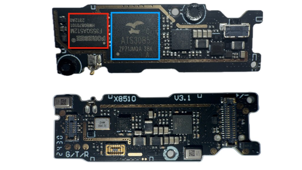
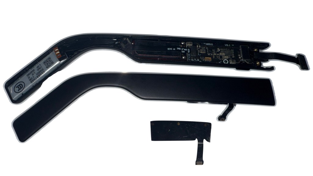
Finally for the main board, we have a dense dual-sided PCB housing an antenna, a variety of ICs, microphones, buttons and connectors – two that I call out specifically for their high BOM impact are the onboard memory in red, a Foresee F35SQA512M NAND Flash Module and an ActionsTech ATS3085 SoC in blue. These are definitely primarily mainland China suppliers that we won’t be seeing in any Meta glasses soon, but it’s interesting to see how intense the competition is for this space despite the overall low volume of units.
Again, shout out to a (much higher production value) teardown from Wen5 just a few weeks ago – go check it out if you want to see a better photographer than me take great glamor shots, while also explaining all the smaller ICs we skipped.

Leave a comment